List of Industries
ADVANCED SOLUTIONS FOR SEMICONDUCTOR
The semiconductor industry is a crucial part of the modern world, providing the backbone for the digital devices we use every day. However, the quality and performance of these devices depend on the materials and manufacturing processes used in the semiconductor industry. As a result, there is a constant need for quality assurance to ensure that these products meet the highest standards.
As a one-stop solution provider for the semiconductor industry, we offer a comprehensive range of products to semiconductor manufacturers. By working with us, semiconductor manufacturers can benefit from a holistic approach to their operations, streamlining their processes, and improving the quality and performance of their products. Our team of experts stays on top of the latest developments in semiconductor technology to ensure we provide the most innovative and effective solutions to our customers.
INCOMING RAW MATERIAL
Material Identification
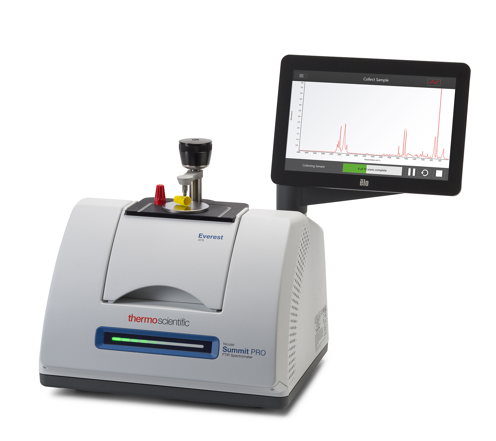
Fourier Transform Infrared Spectrometer (FTIR)
~ Identify the foreign material (bulk sample analysis) present, chemical type.
~ Ensuring the quality of raw materials used in Printed Circuit Boards (PCBs) meet the requirement standards.
~ Checking the Curing Status in Electronic Packaging as uncured process could lead to failure.
~ Analysis of Specialty Gases
Material Identification
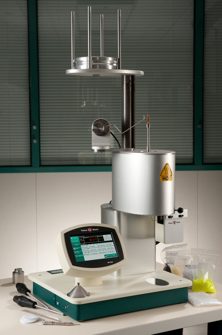
Melt Flow Indexer MP1200
~ Measure the melt flow polymer materials according to all the Procedure A, B, C, D in ASTM D1238 or ISO 1133.
Particle Size For CMP Slurry
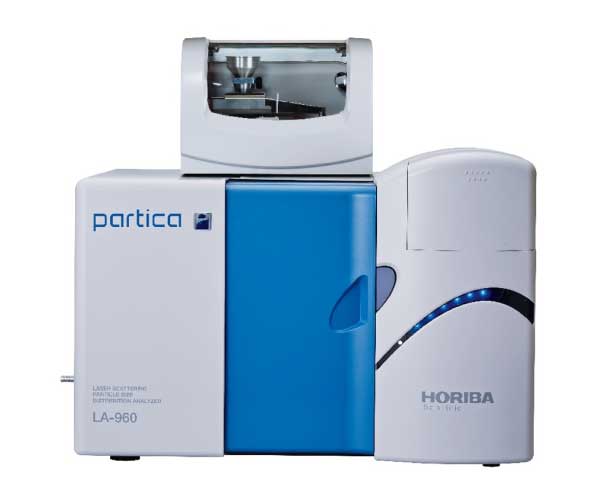
Particle Size Analyzer
~ Checking the particle sizes & distribution for materials used for wafer polishing.
Particle Size For CMP Slurry
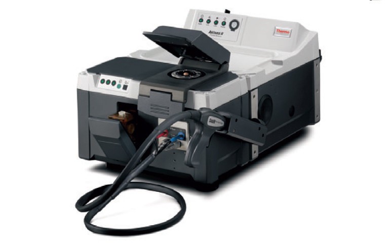
Fourier Transform Near-Infrared Spectroscopy (FT-NIR)
~ Quick analysis to measure the hydrogen peroxide (oxidizer) level in the Chemical Mechanical Planarization (CMP) Slurry
R&D FORMULATION
Thermal Analysis for Product Processability, Product Stability, Process and Curing Optimization
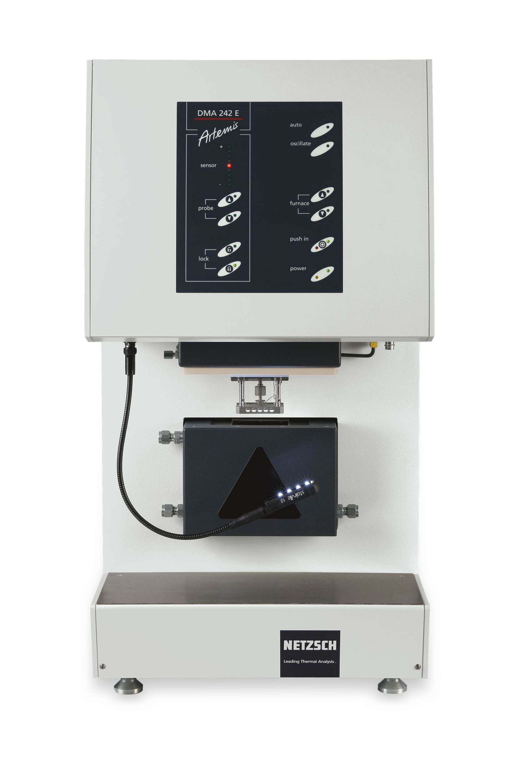
Dynamic Mechanical Analyzer (DMA)
~ A very sensitive technique to obtain the Electronic Boards glass transition temperature (Tg), Storage Modulus & Loss Modulus
Thermal Analysis for Product Processability, Product Stability, Process and Curing Optimization
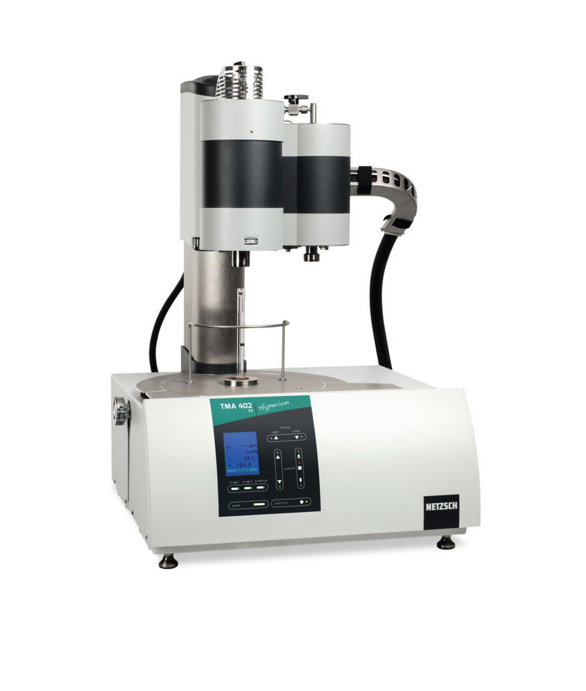
Thermomechanical Analyzer (TMA)
~ Checking the coefficient of thermal expansion (CTE) in Underfill materials to minimize the CTE mismatch between chips and the printed circuit boards (PCBs). Also to measure the glass transition temperature (Tg) for the substrates.
Thermal Analysis for Product Processability, Product Stability, Process and Curing Optimization
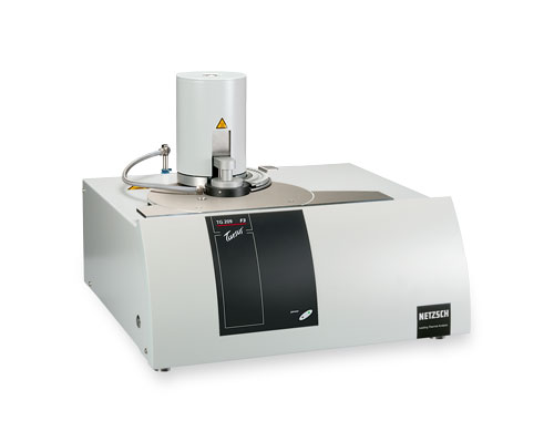
Thermogravimetric Analyzer (TGA)
~ Checking the thermal stability of the materials and also the compositional analysis.
Thermal Analysis for Product Processability, Product Stability, Process and Curing Optimization
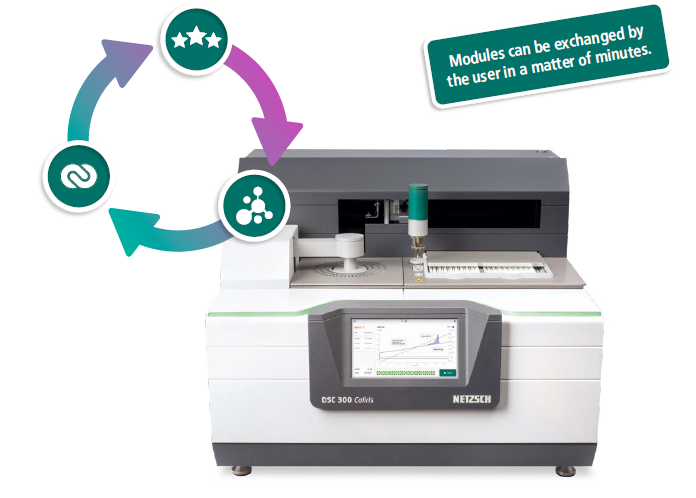
Differential Scanning Calorimeter (DSC)
~ Measure the thermal transition such as melting, glass transition & crystallization. Also used to check the degree of curing for the thermosets material in the PCBs underfill.
Thermal Analysis for Product Processability, Product Stability, Process and Curing Optimization
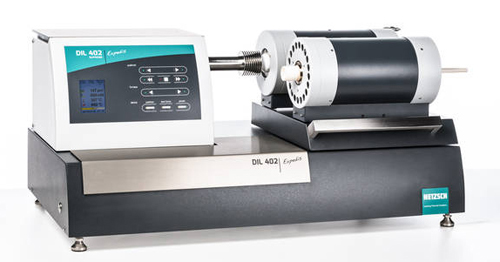
Dilatometer
~Checking the coefficient of thermal expansion (CTE) and glass transition temperature of electronic Circuit Boards substrate
Contact Angle Surface Tension For Plasma Cleaning/Coating
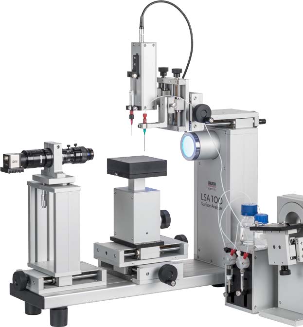
Surface Analyzer
~ The contact angle measurement, surface tension of liquid, surface free energy of substrate are critical to determine the wetting capability of the solution to a substrate such as sensors.
Rheology
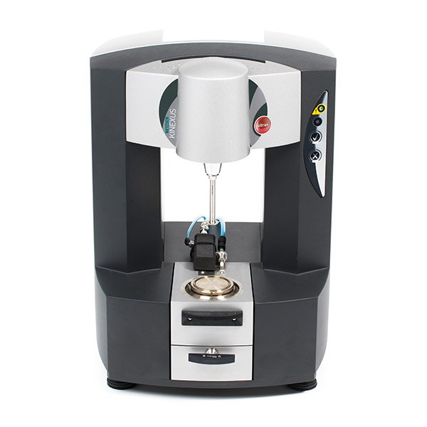
Rotational Rheometer
~ Determine the rheological properties such as the shear viscosity of the polymer coatings that would be applied to substrates.
QA/QC MATERIAL CHARACTERISATION
Failure Analysis/Contamination
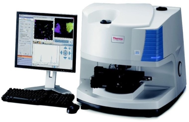
FTIR Microscope
(10 micron spatial resolution)
~ Typically used in the Failure Analysis departments to identify organic contaminations found in the Electronic Packaging, PCB and Displays, either in form of powders/ stains/ foreign particles down to 10 micron size.
Failure Analysis/Contamination
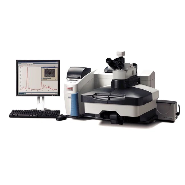
Raman Microscope
(1 micron spatial resolution)
~ Typically used in the Failure Analysis departments to identify Inorganic contaminations found in the Electronic Packaging, PCB and Displays.
~ Analyzing the orientation of screen Protective film by polarized raman.
Failure Analysis/Contamination
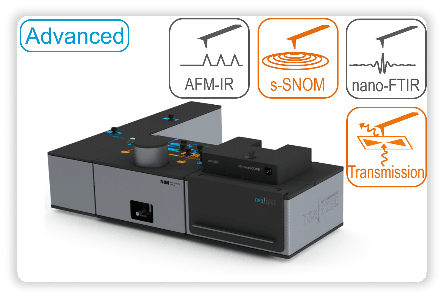
Nano IR Microscope (20 nm spatial resolution)
~ Nano-FTIR spectroscopy performing infrared imaging for chemical identification down to 10nm, and is suited for all classes materials-organics & inorganics
Physical Testing
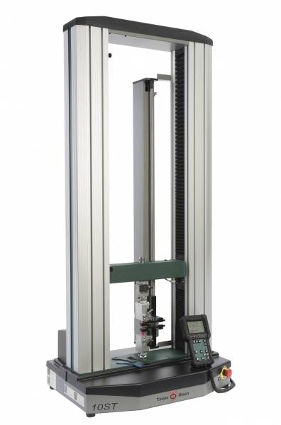
Tensile Machine
~ Capturing the Tensile Strength, Elongation, Flexural Properties, Compression strength for Printed circuit boards
Physical Testing
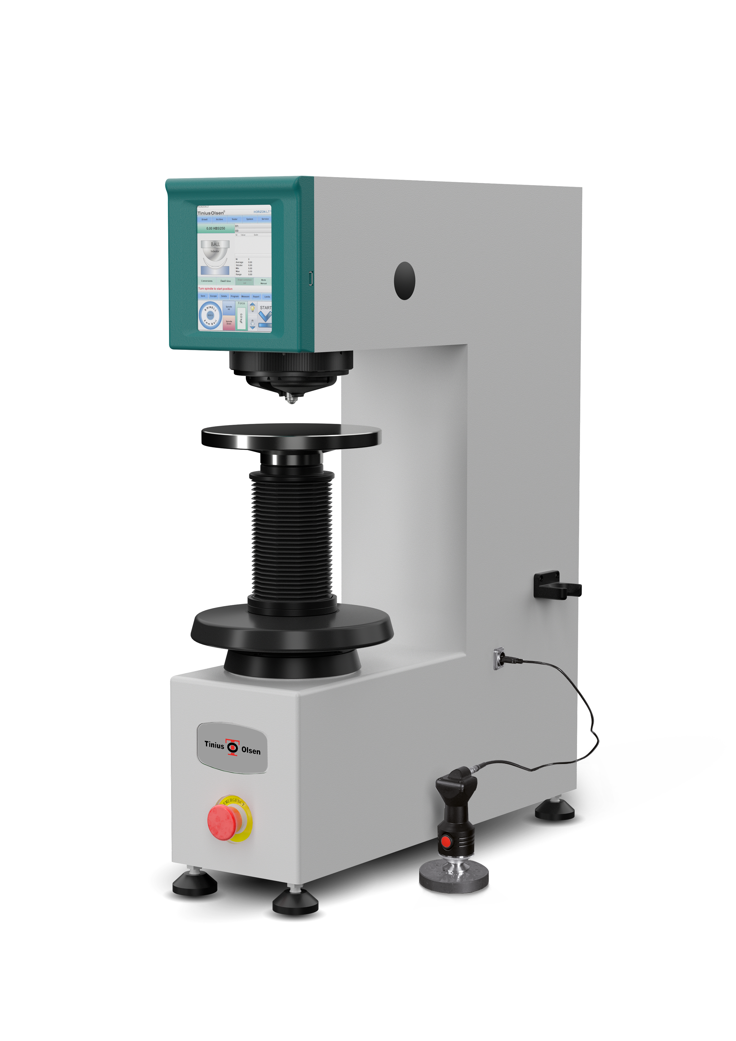
Hardness Tester
~ Measuring the Hardness test for the solder mask on the electronics boards
Chemical Testing for Crosslink density/Curing
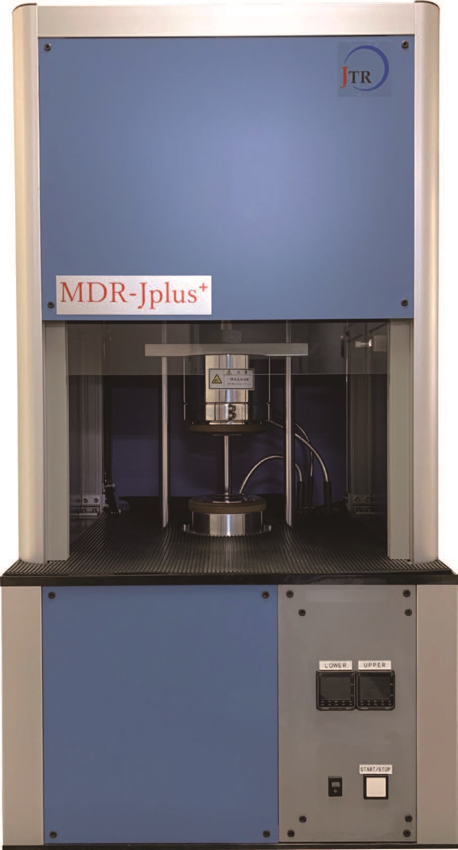
Curemeter/Moving Die Rheometer
~ Measuring the vulcanization process for both hardening behaviour in polyesters resins


